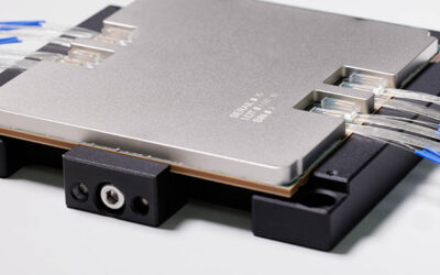
In collaboration with Surfix Diagnostics, PHIX is pleased to offer you a white paper about the wafer level manufacturing of photonic biosensors with integrated active components. As part of this work, PHIX demonstrates flip chip integration of III-V photonic components and NTC thermistors onto a silicon nitride wafer using a state-of-the-art laser assisted heating process.
This process development for the scalable manufacturing of integrated photonic biosensors is part of the PHOTO-SENS project. Using our automated pick-and-place equipment fitted with a custom module for laser assisted heating, we can perform bonding of vertical cavity surface emitting lasers (VCSELs), gallium arsenide (GaAs) photodiode arrays, and NTC thermistors onto a silicon nitride (SiN) photonic platform at wafer level. Part of this process can be seen in action in the video.
After being populated with the active and passive components, a process developed by Surfix Diagnostics subjects the wafer to nanocoating and biofunctionalization. After singulation, through stealth dicing to keep the coatings intact, the hybrid photonic integrated circuits (PICs) will be integrated with microfluids and read-out electronics to form a photonic biosensing platform.
Download our PHOTO-SENS White Paper
Learn more about wafer level manufacturing of photonic biosensors.
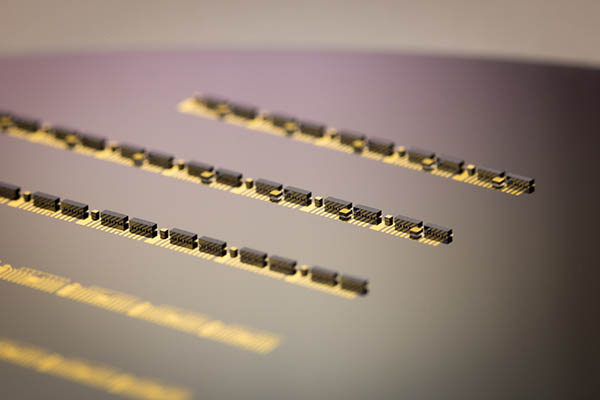
SiN photonic wafer populated with VCSELs, photodiode arrays and thermistors