February 29th 2024
Navigating the complexity of photonic integrated circuit (PIC) packaging already starts at the chip design and layout phase. In this blog series PHIX helps PIC designers take a system-level approach that takes device manufacturability into early consideration. Today, we will discuss how the use of alignment waveguide loops can minimize packaging costs, facilitate PIC characterization and optimize the device’s performance.
The importance of a system-level approach to PIC design
Designing and manufacturing an optoelectronic module based on one or more photonic integrated circuits (PICs) is a challenging and multidisciplinary activity. The complexity of transforming chips into functional devices is often underestimated by designers focusing on the PIC alone. It’s important to understand that making favorable chip design and layout choices early in the project will not only help control the notoriously sizeable packaging costs, but can also significantly increase the performance of the optoelectronic module and accelerate its time to market.
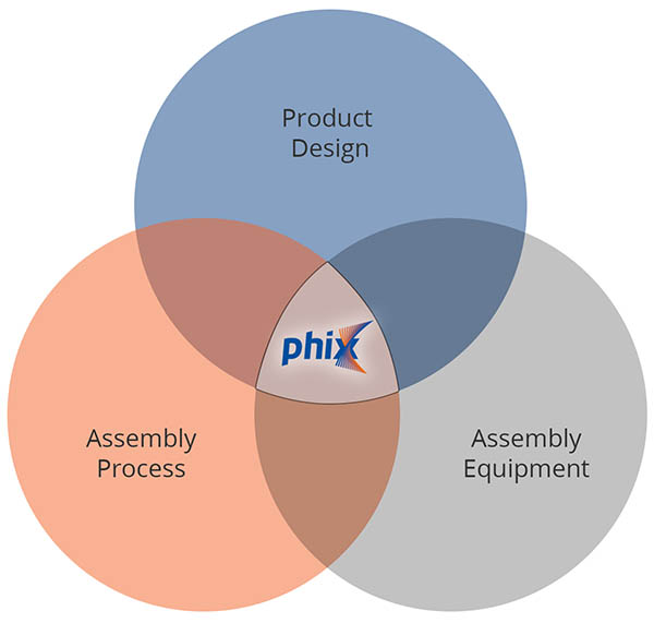
At PHIX we’d like to contribute to the success of your PIC based innovations by encouraging you to take a proactive and system-level approach to PIC design that anticipates and mitigates potential challenges in the assembly process. To help you tap into PHIX’s extensive integrated photonics packaging expertise, we created this blog series and a PIC Design Guidelines document. Involving PHIX early on in the PIC and module design process will bring important process development and manufacturing equipment considerations to the table. As a result of this collaboration your device will optimally balance product performance with cost and ease of scale-up.
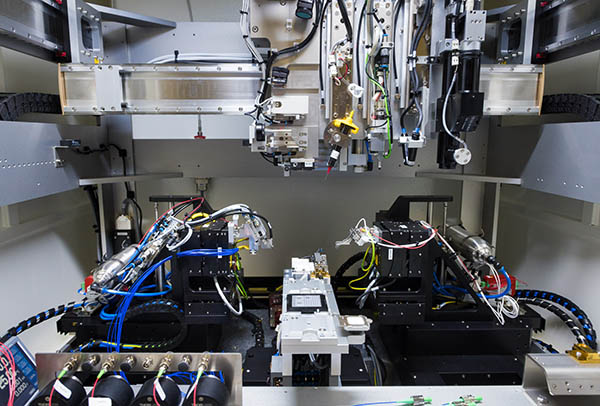
Understanding alignment waveguide loops
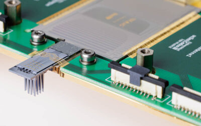
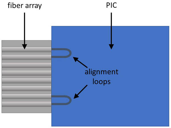
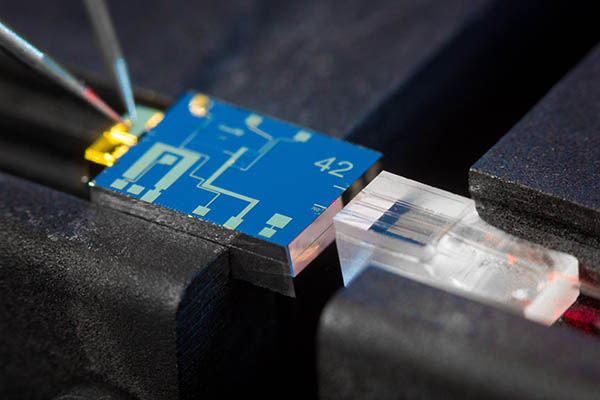
One example of taking a proactive system-level approach to PIC design is the use of alignment waveguide loops. Alignment loops, also referred to as optical shunts, are embedded waveguide loops that are not part of the functional optical structures on a photonic chip. Instead, these extra waveguides enable active alignment routines during the assembly of the optical interface, most commonly between a PIC and a fiber array. PHIX can perform this active alignment on in-house automated equipment, where the optimal coupling position is determined with six degrees of freedom, in combination with calibrated light sources and detectors. Active alignment is critical for achieving the best possible coupling efficiency at the optical interface.
Why alignment loops are essential
While it’s true that the extra chip area and additional fibers needed for these alignment loops add to the cost of the optoelectronic module, let’s look at the consequences of omitting them. Without alignment waveguide loops, active alignment techniques would require the packaging foundry to use probes to activate the functionality of the chip, for example, by driving gain elements and measuring photodiode currents. Using probes instead of alignment waveguide loops has a number of disadvantages:
- These probes are chip-specific, so they would have to be custom-designed and manufactured and cannot be reused for other projects. This would significantly raise the non-recurring engineering (NRE) cost of prototype packaging. Incorporating alignment waveguide loops postpones the investment in such customized tooling and provides more flexibility independent of the chip design.
- Reliable assembly process control monitoring cannot be performed without waveguide loops, because if the on-chip optical signal is activated using probes, the assembly performance would convoluted with the performance of the PIC.
- The heat and radiation used for epoxy curing during assembly may temporarily destabilize the processes on the chip. Reliance on probes makes it difficult to track the waveguide’s position during curing.
- The probes may scratch bond pads, making wire bonding more challenging later in the packaging process.
- Using functional structures on the chip for alignment requires PHIX to have some knowledge of the chip’s functionality, which may require disclosure of intellectual property that the PIC designers are not comfortable to share.
- The use of alignment waveguide loops can help with PIC characterization. Two loops of unequal length at the fiber array interface allow a first-order estimation of the waveguide propagation loss to be made.
Although waveguide alignment loops occupy space and add some cost to the fiber count, they compensate for this by making the manufacturing process much more robust and affordable. This is of particular importance for PICs that originate from multi-project wafer (MPW) runs and are intended for low to medium-volume device manufacturing. For high-volume applications where the PIC design is finalized and the investment in custom tooling and processes is warranted, active alignment without waveguide loops, or even passive alignment, become serious alternatives. Making this consideration based on the development stage of the project and by weighing costs, performance and manufacturability, is precisely what taking a system-level approach to PIC based module design is all about!
How PHIX makes your projects succeed
PHIX is happy to assist your system-level approach towards a successful PIC-based device. A great first step is to study our Design Guidelines for PIC Packaging document. Once you are ready to start designing, please involve PHIX early on. Our selection of standard package types gives a nice overview of some of the housings that you can use for your module. Some housings are specifically designed for protoype packaging, while others also support volume packaging.
Download our Design Guidelines (.pdf)
To help you optimize your PIC design for low-cost and low-risk packaging and select the most suitable standardized package type, we offer you our PHIX Design Guidelines document as a free download.