
Market: Datacom / CPO
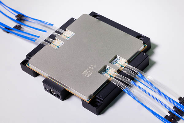
The rise of integrated photonics in datacom
The evolution of data center infrastructure has long been driven by advances in optical interconnects. Over the past decades, integrated photonics has replaced discrete optical solutions, which enabled exponential growth in data rates while improving energy efficiency. This has transformed how hyperscale and enterprise data centers operate today.
The industry progressed toward the widespread adoption of small form pluggable (SFP) optical transceivers, where the electrical and mechanical interface were standardized. This enabled rapid development of different photonic solutions into a common interface. Datacenter builders could select the best interconnect solution for their datacenter architecture. Photonic integrated circuits (PICs) got introduced as a solution to increase bandwidth, lower power consumption, and integrate more closely with electronics. This shift enabled wafer-scale manufacturing, tighter integration of optical functions, and a steady climb to 100G, 400G, 800G, and beyond. Techniques like wavelength-division multiplexing (WDM) and advanced modulation schemes further increased bandwidth without significantly expanding the footprint.
However, the rapid rise of artificial intelligence (AI) has introduced a new scaling challenge. AI clusters demand massive bandwidth between large groups of computer processors (xPUs), memory, and switches. Traditional pluggable optics, where optical modules sit at the switch front panel, introduce long copper traces between the electronics and the optical engine. At speeds of 400G, 800G, and beyond, these traces introduce high ohmic resistance. This results in high signal losses, which call for larger and more power-hungry drive and error correction circuits.
As a result of this challenge, the industry is reducing the electrical distance between the switch electronics and the optical engine. This transition is happening in stages, from traditional pluggable optics to linear drive pluggable optics (LPO), near-packaged optics (NPO), and ultimately co-packaged optics (CPO). Each stage comes with a new set of packaging challenges, which PHIX can play an important role to tackle.
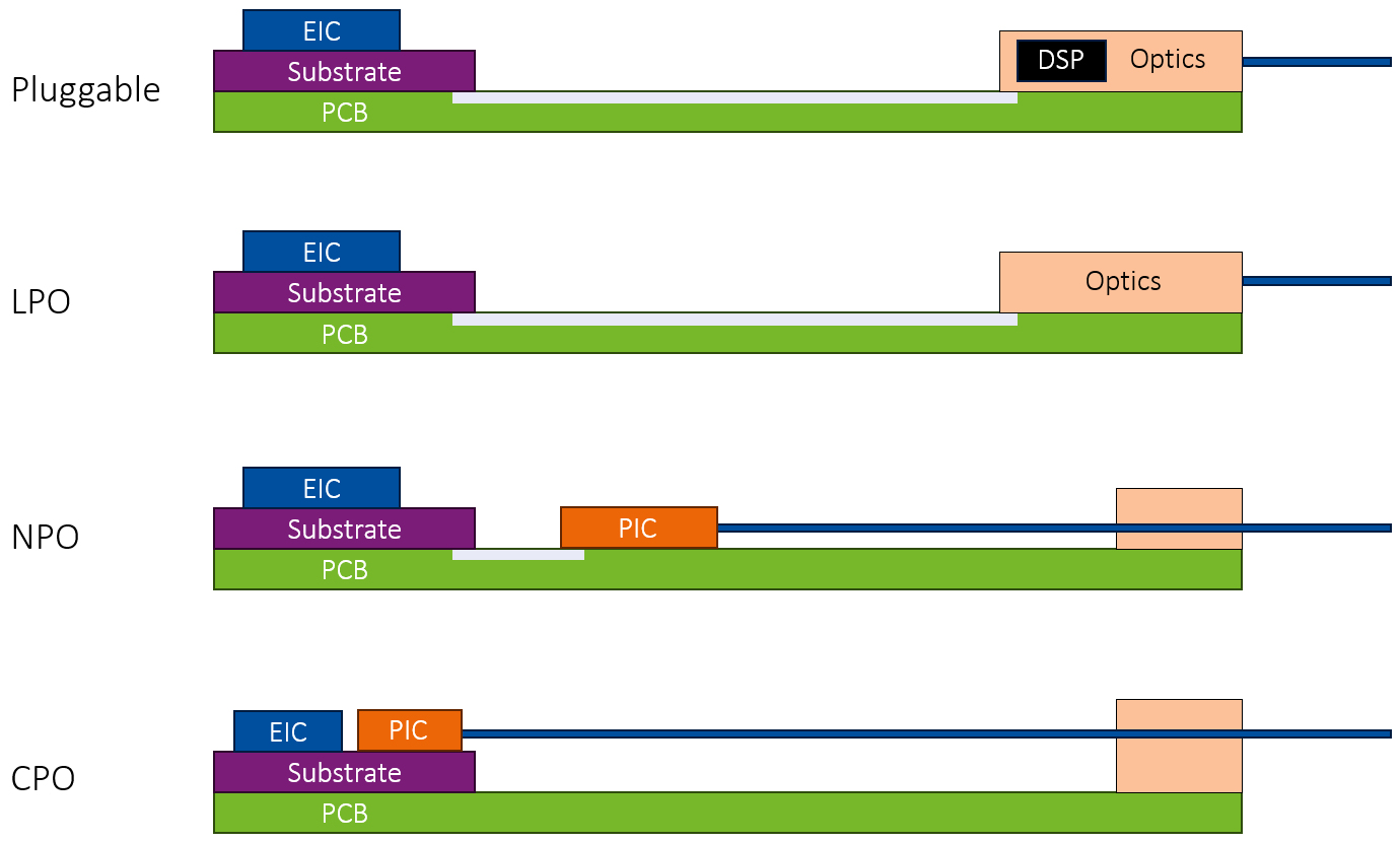
Staged evolution of pluggable optical transceivers to co-packaged optics
The migration path from pluggables to LPO, to NPO, to CPO
Rather than a single disruptive shift, the move toward CPO is happening incrementally:
- Pluggable optical transceivers remain dominant due to their flexibility and ease of repair and upgrade, but are becoming increasingly power-inefficient at higher speeds.
- Linear drive pluggable optics (LPO) simplify digital signal processing (DSP) requirements, reducing power consumption and latency.
- Near-packaged optics (NPO) bring the optics closer to the application-specific electronic integrated circuit (ASIC), shortening electrical traces.
- Co-packaged optics (CPO) fully integrates optics within the switch package.
The staged evolution from pluggable transceivers to CPO introduces new packaging complexity with each step. As an independent photonics packaging foundry and NPI partner, PHIX can play a critical role across the entire migration path, from LPO and NPO to full CPO deployment.
Addressing challenges across architectures
The added performance and lower energy consumption that the transition towards CPO brings comes at a cost of several design and manufacturing challenges. Technical solutions that address these are scrutinized by strong market demands for reliability and low cost.
Optical coupling at scale
The high bandwidth of architectures evolving toward CPO requires high channel count fiber to chip interfaces with submicron alignment tolerances. Novel approaches to enhance the “beachfront” utilization and enhancing fiber density are being exploited. This calls for fiber coupling solutions that provide minimum losses, scale well with channel count, are pluggable for ease of repair, and enable high-yield manufacturing.
For the adoption of innovative new pluggable fiber interfaces into our assembly processes, also in combination with 3D integration platforms such as TSMC’s COUPE and GlobalFoundries’ SCALE, PHIX is in close contact with market leaders such as Corning, Senko, and Molex.
Heterogeneous integration
Combining PICs, III-V lasers, and advanced electronics at high density requires high-precision 3D assembly. The reliability of these interconnects is challenged by thermal and mechanical incompatibilities between the various components and the accuracy with which they get assembled. Laser and semiconductor optical amplifier (SOA) integration allows for local generation and amplification of the optical signal, while close integration of the electronics enables high signal quality. While this technology matures, other materials like thin film lithium niobate (TFLN) and barium titanate (BTO) are on the verge of a breakthrough to further increase the frequency and lower the power consumption. All of these are reducing the power at the core of the compute system.
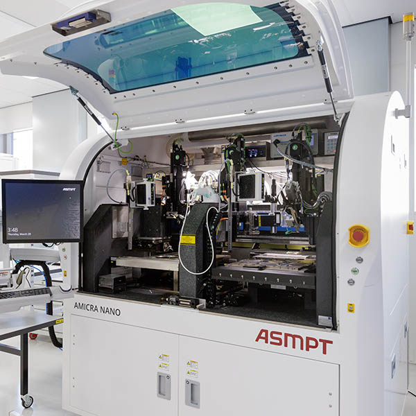
Ready to tackle the most demanding integration challenges, PHIX owns the world’s most accurate die bonding equipment, the ASMPT Amicra Nano. Aside from its class leading positioning accuracy of 0.2 um, this machine performs die bonding at wafer level, at high speed and high automation level.
Subsystem serviceability
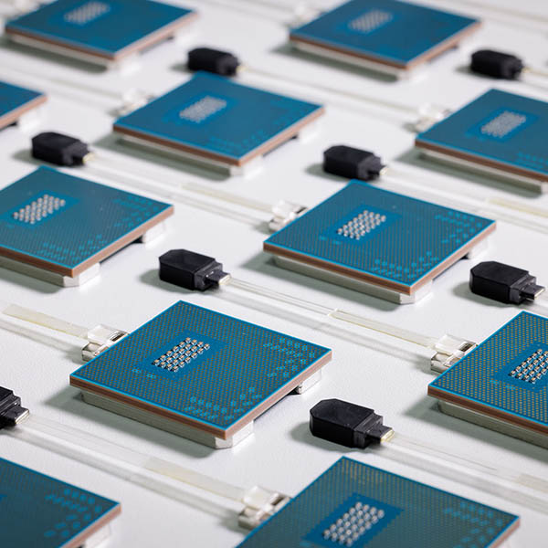
Tight integration of optical and electronic components imposes a challenge on the serviceability of devices. Non-detachable assemblies make failures more difficult to isolate and repair, and risk that large costly subsystems need to be scrapped.
Serviceability is not just an issue in the field, but also in manufacturing. Even with high yields on the individual components and assembly processes, the likelihood of a faulty subsystem increases exponentially with the number of integrated components. Avoiding scrapped subsystems by replacing individual parts can therefore make a significant impact on the cost-effectiveness and sustainability of CPO devices.
PHIX contributes to device serviceability by assisting in the adoption of the aforementioned pluggable fiber interface innovations.
Manufacturing scalability
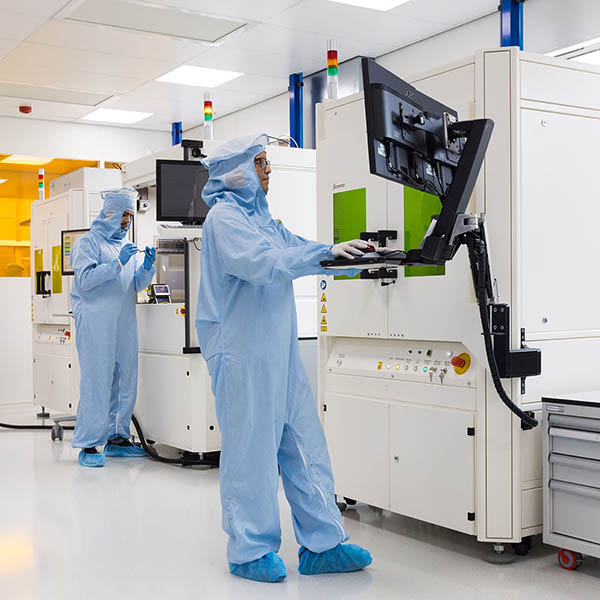
Where PIC fabrication costs diminish as device manufacturing is scaled to high volumes, the cost and throughput speed of packaging is becoming a bottleneck. This throughput limitation already begins at die testing and continues for each subsequent process step that requires cycle time optimization. A parallel challenge to scalable and repeatable packaging of novel integration architectures is the limited standardization and high ecosystem fragmentation.
As a partner within the Advanced Photonics Coalition, PHIX is actively contributing to the establishment of standards for CPO manufacturing. We adapt our technology roadmap to the projections of our customers and the integrated photonics market, and invest in equipment, facilities, and human resources ahead of the curve. We are working with several very large-scale manufacturing partners to enable seamless production scaling when ramp-up rates or volumes exceed our in-house capabilities.
Thermal management
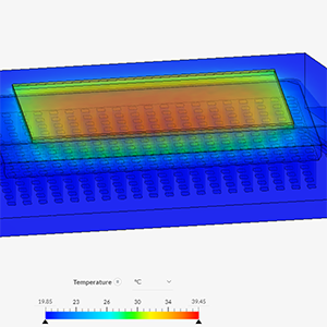
As optics move closer to high-power ASICs, the risk of wavelength drift due to thermal crosstalk increases significantly. If lasers are integrated within the same package, the higher temperatures may reduce their efficiency and lifetime. These issues require advanced cooling solutions operating at package level.
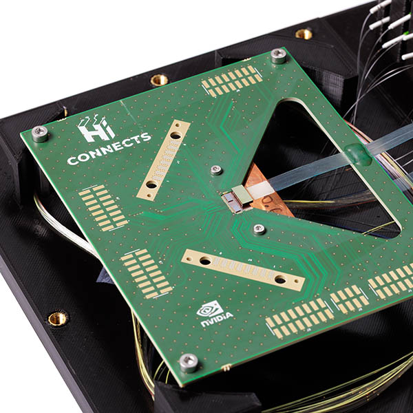
As an integrator of optical and electrical components into high-performance and robust optoelectronic modules, PHIX has an extensive track record in thermal management. Our engineers are experts at thermal design and simulation, and their involvement in various international research consortia, such as HiCONNECTS, keeps them on the cutting edge of complex system-level module design.
Accelerating New Product Introductions (NPIs)
The transition to CPO represents a fundamental shift in how data centers are designed and scaled. Driven by AI, this transition is as much about packaging innovation as it is about photonic integration. In this landscape, packaging is no longer a backend process, but a core enabler of system performance and scalability.
PHIX supports NPI for hyperscalers by:
- Harnessing extensive cross-architecture expertise in fiber-to-chip coupling, flip-chip integration, light source assembly and scalable manufacturing for LPO, NPO, and CPO.
- Taking a system-level approach to co-design, process development, and manufacturing early in the development, balancing performance, cost, and lead time.
- Providing proven photonics assembly processes.
- Enabling a smooth path from prototyping to high volume production.
With this approach, PHIX enables companies to move from concept to deployment with confidence, turning CPO from a promising architecture into volume.